Would watching the hockey playoffs be more fun if you could see the arena projected in three dimensions on top of your coffee table, the players just 10 centimetres tall and visible from all angles? Imagine that same kind of holographic technology applied to medical imaging, where a radiologist could walk the surgeon through a 3D projection of a tumour that needs to be removed. Or consider how a 3D projection could be used to facilitate a conversation between an engineer designing the newest jet engine and the maintenance experts providing feedback on where to locate the bolts for easy access.
These kinds of powerful new tools for communicating information are not far off, and one Newfoundland company is tapping into sophisticated research tools to help lead the charge.
Avalon Holographics, headquartered in St. John’s, collaborates with nanofabrication facilities at both the University of Waterloo and the University of Alberta to create and test nano-sized devices for holographic display technologies. The devices will ultimately produce a life-like display that is “nearly indecipherable from the real thing,” says the company’s president, Wally Haas.
In the past, holograms have relied on a system of mirrors to manipulate light and create a 3D effect, explains Greg Holloway, a researcher at Waterloo’s Quantum NanoFab facility. But a much higher-fidelity 3D projection can be created using nano-sized structures on the scale of the wavelength of light. When light is shone on them, the structures cause the light to bend, yielding a 3D projection; it’s a little bit like an optical music box.
The structures are essentially tiny pillars mounted on glass that Holloway sculpts into the desired shape using electron beam lithography, which uses a high-energy beam of electrons to burn away material. The resulting device is 100 microns in size, barely visible.

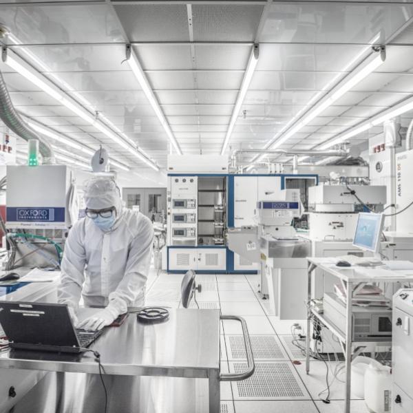
Nine of the company’s 40 employees also work on developing holographic devices at the nanoFab Fabrication & Characterization Centre at U of A, which is the country’s largest clean room open to industry use.
Haas says these research facilities are indispensable to his company’s success. The precision of the electron beam lithography equipment at Waterloo, for example, allows Avalon to advance their technologies further than they otherwise could, says Haas. Machines like it are not widely available and can be “expensive and finicky” making the capability and expertise at Waterloo’s facility that much more valuable. And Haas doesn’t mince words about the value of the U of A facility. “Without it we’d shut down. We are lucky to have access to its size and capability, and if there were more facilities like that in Canada, you’d have more start-ups like ours.”
Although there is still work to be done before we can watch the hockey finals in 3D, Haas says he’s confident in the devices his company is building. “It’s not a question of technology anymore in my mind,” he says, but more a question of the time and expense required to be ready to commercialize it. But it is just that, he says — a matter of time. “We are on our way.”


